The big picture: Hopper is a reference to Grace Hopper (above), a pioneer of computer science and a Navy officer. Among her achievements was the co-creation of UNIVAC, the first fully electronic computer; the co-creation of COBOL, the first enterprise programming language; and the coining of the term “bug” to describe a computer malfunction.
Nvidia first applied to trademark the name Hopper in 2020, and is rumored to be the successor to the Ampere architecture since.
However, Hopper is also the name used by Dish Network for some of its products. Their use of it is in reference to a kangaroo literally hopping around. In April last year, they contested Nvidia’s trademark of the name, claiming that it infringes on their trademark of it in relation to telecommunications services.
Nvidia’s trademark of the name is broad. It mentions telecommunications services once, in the context of providing software (it describes data services 54 times, artificial intelligence 23 times, and gaming 17 times).

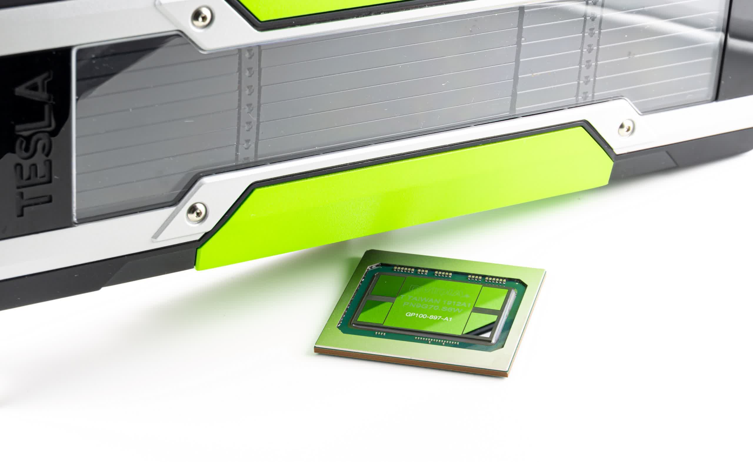
An Nvidia P100 with its GPU removed. Hopper will target the same server markets as the P100 did but will be several times more powerful.
Since legal proceedings began, the companies have requested five suspensions to negotiate a settlement. The current suspension will expire on February 22, which doesn’t leave enough time for a court case if Nvidia wants to announce the Hopper architecture at GTC 2022 in March.
It seems likely that it would want to, given that it’s been two years since they announced the Ampere architecture. Since then, both AMD and Intel have announced their superseding architectures. According to some leaks, Hopper will be an enterprise-focused architecture, like the older Volta architecture.
A reliable leaker recently shared that he believes the GH100 processor, based on the Hopper architecture, will have a die size of almost 1000 mm2. It could have up to 288 SMs, or 2.6 times more cores than the Ampere-based GA100 processor.
Image credit: US National Archives and Record Administration, Fritzchens Fritz

