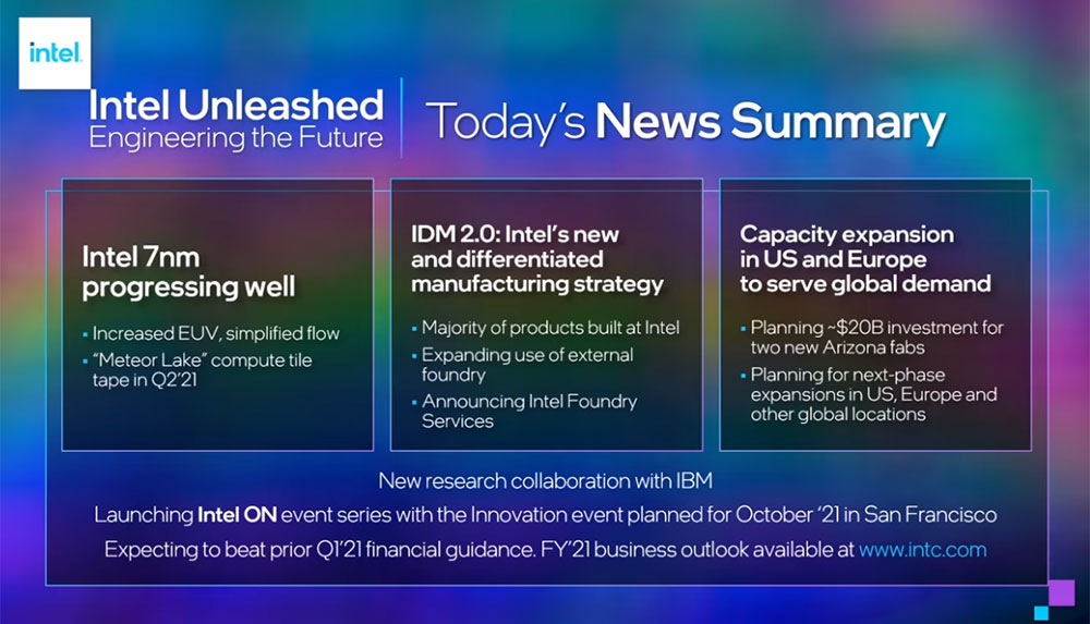
Intel’s Engineering the Future webcast has wrapped up, and it was an info packed event with lots of news for engineers, analysts, and enthusiasts. While Intel spoke at length about its IDM 2.0 strategy and investment plans, the setting up of Intel Foundry Services (IFS), and re-start of an IDF-alike annual event dubbed Intel ON, it also offered some tasty morsels for we PC enthusiasts.

IDM 2.0 is going to be pretty important for Intel in the next few years. This is how Intel has set out its stall to reaffirm its commitment to being a fully vertically integrated operation from design to shipping CPUs. Thus, it has announced significant investment in new fabs, especially in the US, that it will happily use external foundries when needed, and that IFS will use its in house state-of-the-art foundry facilities to output custom chip designs using Arm, RISC-V, as well as x86 designs.
Intel’s new CEO Pat Gelsinger provided an update on how the current 10nm processor business is progressing. The currently shipping Tiger Lake CPUs for laptops are claimed to be selling well. For example, 30 million TGL chips have shipped, and they can be found in 150 partner laptop designs. It is further noted that 100 of those designs are premium Evo certified products.
Alder Lake chips are said to be sampling to customers, which might explain the various leaked benchmarks and so on. After Rocket Lake-S arrives later this month this will be keenly awaited by PC enthusiasts and DIYers as it brings a number of significant advancements to the Core processor line for the first time in a long time (10nm, up to 16 hybrid cores, DDR5, PCIE 5.0 and more).

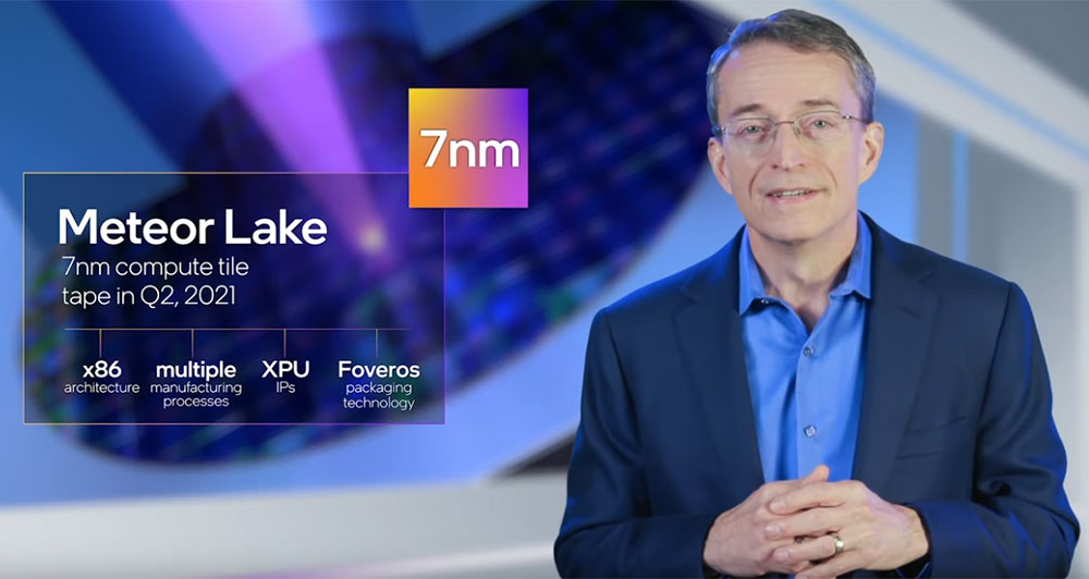
Intel’s 7nm Meteor Lake processor development will shortly reach a milestone. The tape-in (design IP verification) is expected to complete in the next few months (sometime in Q2 this year). Gelsinger confirmed that these processors will embrace the x86 architecture, feature multiple manufacturing processes to form the SoCs, include XPU IPs (AI accelerators, DSPs, etc), and make use of Intel’s Foveros die stacking tech in their construction.
Other important news going forward is likely going to be Intel’s new research partnerships with Microsoft and IBM, and the annual autumnal Intel ON innovation events starting this year in San Francisco.

