Updated
The goal, we’re told, is for Intel to return to the “tick-tock” manufacturing model of its glory days.
Today’s Best Tech Deals
Picked by PCWorld’s Editors
Top Deals On Great Products
Picked by Techconnect’s Editors
On Tuesday, newly minted Intel chief executive Pat Gelsinger outlined his vision for returning Intel to greatness: a manufacturing strategy called “IDM 2.0” that will impact Intel’s development of 7nm chips, including the upcoming Meteor Lake.
At its heart, Gelsinger’s IDM 2.0 is about fabs: building two new fabs in Arizona to help alleviate worldwide semiconductor supply concerns; establishing a brand-new Intel Foundry Services business to sell chips from those fabs to other customers; and, conversely, creating a culture where Intel will turn to other chip foundries to manufacture products that it can’t manufacture itself.
Gelsinger made clear that Intel’s goal is to continue manufacturing the majority of its products internally, but that it will turn to other foundry partners where necessary. Gelsinger said Intel’s working hard to streamline and simplify its chip recipe to accelerate its roadmap. In terms of its consumer roadmap, Intel expects to solidify the design of the compute tile of its first 7nm CPU, code-named Meteor Lake, in the second quarter of this year, before it officially launches in 2023.
“As I hope you’ve gathered, Intel is back,” Gelsinger said. “The old Intel, is now the new Intel, as we look to the future. We are excited about the things we are laying out.”
Gelsinger, who once was the face of the popular Intel Developer Forum (IDF), also revealed that Intel is bringing back the “spirit” of IDF with the launch of Intel On, a new industry event series. Intel also plans an Intel Innovation event in October in San Francisco that sounds like it could be a replacement for IDF.
 Intel
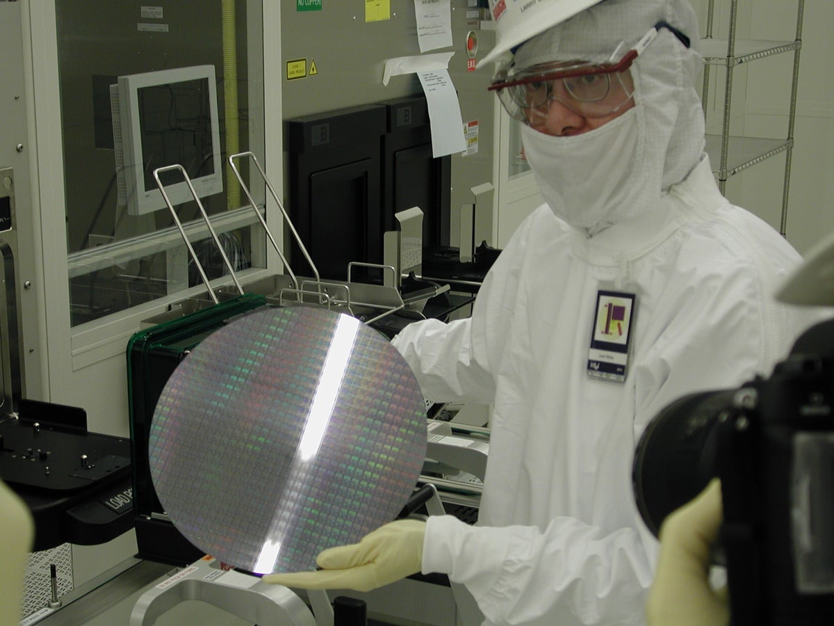
Intel An Intel manufacturing worker holds a chip wafer.
What Intel’s new plans mean for PCs
Gelsinger’s plans were unveiled five weeks after he took office on February 15. Gelsinger was named Intel’s new chief executive to replace Bob Swan in January. Intel named Swan as a “temporary” replacement after Brian Krzanich unexpectedly stepped down in 2018, following the revelation of a consensual relationship with an employee.
Gelsinger is a thirty-year veteran of Intel who worked closely on the development of USB and Wi-Fi. When his CEO role was announced, Gelsinger seemed to promise a return to the good old days as he described learning his craft at the feet of past Intel greats such as Gordon Moore and Robert Noyce. His goals, Gelsinger said at the time, included making Intel’s manufacturing more agile, to design great products, and to execute quickly on those plans.
Those statements came as Intel continues to be stuck selling chips based on an aging 14nm process node, an inertia that contrasts sharply with the disciplined “tick-tock” cadence of chip architecture advances that Intel had adhered to for decades. Gelsinger said that originally Intel designed its 7nm process with limited use of Extreme Ultraviolet lithography, a manufacturing technology. That made manufacturing more complex, he added, and eventually proved to be a mistake, delaying Intel’s manufacturing roadmap. Gelsinger said Tuesday that Intel believes that they have solved those problems.
Intel says it’s serious about reviving that regular “tick-tock” pace, but currently Intel’s manufacturing is still stuttering. While the company’s 10th-gen Ice Lake Core chips were fabricated on 10nm, the upcoming Rocket Lake-S desktop chips mark a return to the older 14nm process.
The 7nm Meteor Lake generation will begin “tape in”—a preliminary manufacturing stage—in the second quarter. Gelsinger said that it will include a “breakthrough” new X86 architecture and multiple manufacturing processes, all assembled inside a single package. However, Meteor Lake as a finished product won’t be released until 2023.
Gelsinger also said that Intel’s 11th-gen “Tiger Lake” core has shipped 30 million units. Alder Lake, the next modular Intel CPU, has begin sampling to customers.
New fabs and foundry services
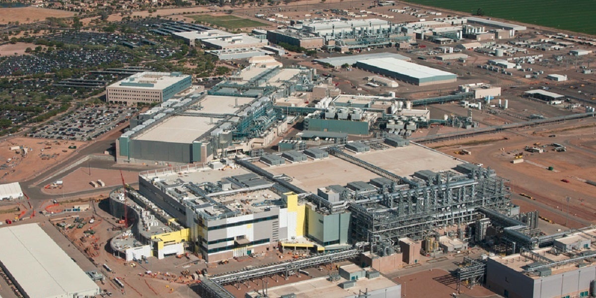
The two new fabs that Intel plans to build will be one of the first steps in Intel’s IDM 2.0 vision. They will be part of Intel’s existing Ocotillo facility in Chandler, Arizona. While Intel provided few details on the fabs, the company said they’d be designed on “the advanced node,” which means Intel’s leading-edge process technology. They’re expected to come online in 2024, Intel sources said.
 Intel
Intel Intel’s Fab 42.
It isn’t clear how much of Intel’s manufacturing capacity available today will be made available to third parties, or how quickly Intel can begin manufacturing products for those customers. What is clear is that the electronics industry is facing a dearth of semiconductors across the board, with Samsung, Honda and Volkswagen warning that a limited supply of chips could impact their ability to manufacture phones. Samsung, for example, reportedly can’t get enough processors from Qualcomm for its low-end phones.
Intel’s new Intel Foundry Services will offer design services that incorporate processor technologies that Intel hasn’t traditionally touted: the open-source RISC-V architecture, but also Arm. Intel is a current Arm licensee, but it hasn’t developed an Arm CPU since the StrongARM chip was discontinued in the early 2000s. Intel also said that it could provide X86 cores for customers to use, too, though it wasn’t clear which cores or under which conditions.
We’re told, though, that Intel Foundry Services will be run independently under Randhir Thakur, and that decisions and intellectual property Intel’s foundry business brings in won’t necessarily affect Intel as a whole—this isn’t a signal that Intel will enter the ARM processor market, in other words.
All of Gelsinger’s initiatives won’t come cheap. Intel said that its IDM 2.0 manufacturing plans will cost the company about $20 billion, though it will create 3,000 high-tech jobs at Intel and thousands more in the surrounding communities, the company said.
Under the hood: Packaging matters, too
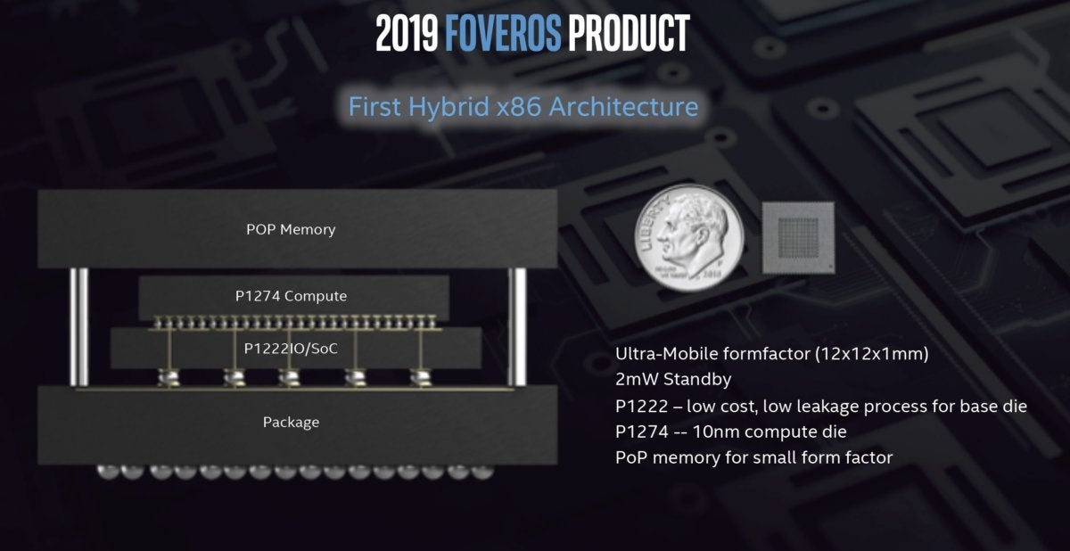
Designing and building a CPU has also become much more nuanced, and Intel’s IDM 2.0 plans take that into account, too. Intel’s hybrid Lakefield chip and the upcoming Alder Lake CPU lean heavily on Intel’s Foveros packaging technology, which allows chip traces to run up and down in three dimensions, shrinking the necessary space that they require. Because of this, processor design has become much more modular, with Intel now referring to different parts of the CPU as “tiles” that can be pieced together.
The IDM 2.0 plan supports this in two ways. For one, Intel and IBM today announced plans for an important research collaboration focused on creating next-generation logic and packaging technologies, working together in Intel’s Oregon and IBM’s New York labs.
Beginning in 2023, Intel said it would begin tapping third-party foundries for manufacturing—not design—help, “for a range of modular tiles on advanced process technologies, including products at the core of Intel’s computing offerings for both client and data center segments.” Intel made clear that it’s already using foundries for some of its needs already, from communications to graphics. Now, it presumably plans to use those foundries, such as TSMC and GlobalFoundries, to help accelerate the more valuable products it would normally manufacture itself, probably to accelerate its manufacturing timetable.
 Intel
IntelA cross-section of how Intel’s Foveros packaging technology works.
At this point, however, it’s unclear what those “tiles” will include, and what products they’ll impact. They will include “leadership” CPUs, we’re told, which will be manufactured on external foundries. That could lead to more supply, potentially lower prices, and more availability of Intel products.
Gelsinger’s message Tuesday leans on manufacturing as the solution to its challenges, but we’re also told that Intel will have plenty to talk about in terms of products and improved design in the future. We’ll see what more the Gelsinger era of Intel holds in store over the coming months.
This story was updated at 4:57 PM with additional detail.
Note: When you purchase something after clicking links in our articles, we may earn a small commission. Read our affiliate link policy for more details.
As PCWorld’s senior editor, Mark focuses on Microsoft news and chip technology, among other beats.

